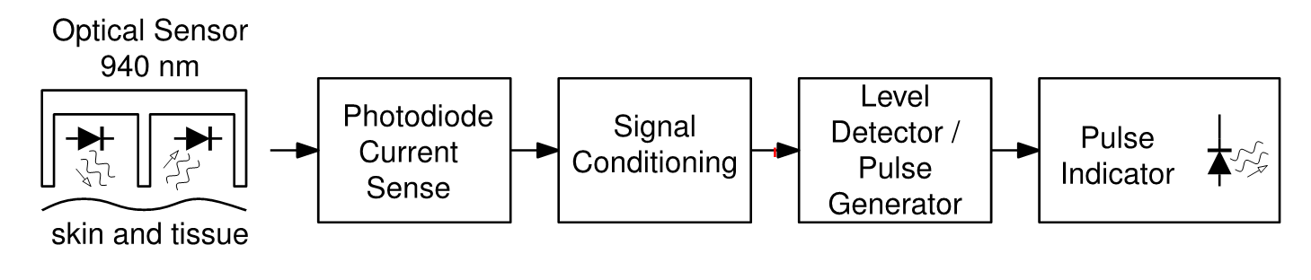
An amazing undegraduate microelectronic circuit design project. The object of this design is to detect the heart rate pulse of human beings. The design flow is given in Fig. 1.
The explanation for the design flow is as follow:
Optical Sensor, Low-pass TIA and Signal Conditioning Circuit
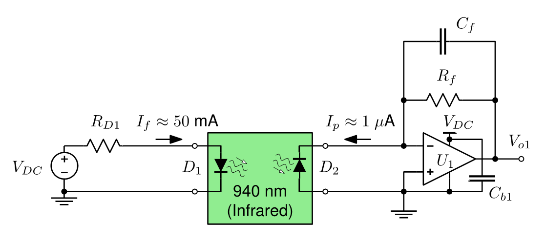
Fig. 2 shows the circuit topology of the optical sensor and low-pass TIA. The optical sensor consists of IR emitter D1 and IR receiver D2 that will be used to attach to the skin and detect the heart rate pulse from the artery through PPG. The signal will be in current mode, which will be transformed into voltage signal through TIA that has a low-pass response, whose cut-off frequency will be determined by the feedback resistor Rf and capacitor Cf.
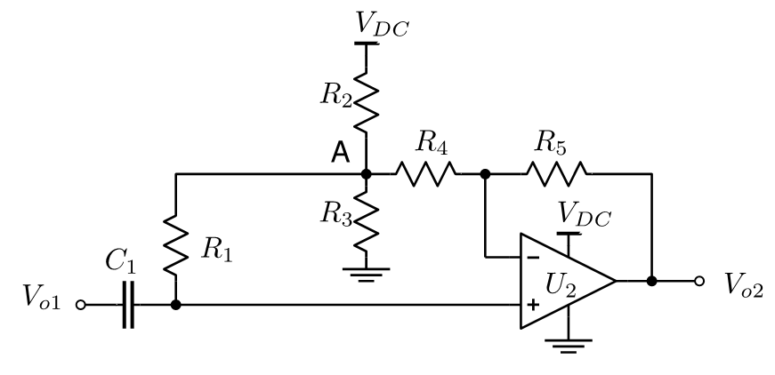
The voltage pulse signal is then passed to the signal conditioning circuitry that consists of a active high-pass filter with gain, shown in Fig. 3. The DC bias resistors R2 and R3 set up a voltage divider and establish the analog ground to the non-inverting amplifier. C1 and R1 establish the high-pass cutoff frequency; R4 and R5 determine the AC signal gain of the filter.
The TIA and signal conditioning circuitries are simulated in LTSpice; you can download the simulaiton file to see the output response, which assumes you have LTSpice installed.
Comparator and Pulse Generator
In order to generate more readable signal that can more easily reflect the heart beat pulses, it will be desirable to convert analog signal to digital pulses. Comparator here does this job, functioning as a simple 1-bit ADC, whose topology is given in Fig. 4. The comparator in this design is a bit different to the genearal comparator as it has a decision-making region bounded by the upper and lower threshold voltages, whose values are determined by R8 and R9.
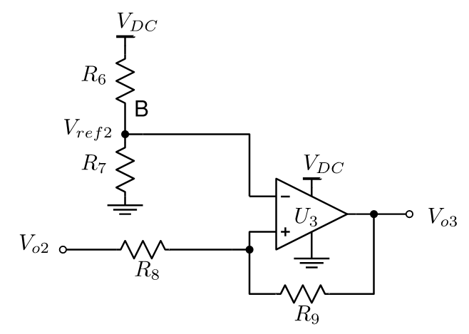
The comparator like this is sometimes also called Schmitt Trigger. Its voltage-transfer-characteristic (VTC) plot is given in Fig. 4. Here, Vref is the reference voltage that sets the mid-point of the decision region; VTH is the upper bound, and VTL is the lower bound. As one can see, the reference voltage is usually set as the mid-point of the DC voltage supply. The way to solve R8 and R9, can be easily done through KCL rule, namely when Vo2 equals to VTL for instance, there is:
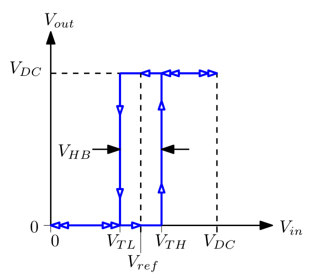
It is also important to select appropriate hysterisis band (decision region) of the Schmitt Trigger that determins the values of VTH and VTL.
The pulse generator consists of a edge-trigger circuit that is essentially a RC-differentiator (I encourage you to see here for more details on RC differentiator/integrator, and RL differentiator/integrator) together with a diode as a rectifier. Then the edge-triggered signal is passed to a monostable multivibrator followed by a LED driver as the visible heart pulse indicator, which will blink one an edge is detected from the optical sensor front-end. The whole module is provided in Fig. 6.
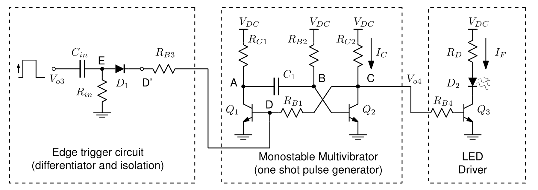
Specific explanations here will be given to the monostable multivibrator.